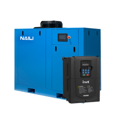
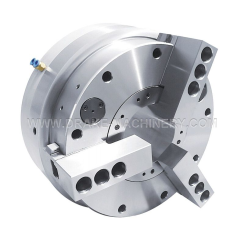
High-speed stacked chip die bonder
High-Speed Stacked Chip Die Bonder: Precision Engineering for Advanced Semiconductor Packaging
Product Description
High-Speed Stacked Chip Die Bonder: Precision Engineering for Advanced Semiconductor Packaging
You will get efficient and thoughtful service from Top Leading.
The High-Speed Stacked Chip Die Bonder is a cutting-edge solution designed for high-efficiency semiconductor packaging applications. Tailored for businesses in the electronics industry, this die bonder seamlessly enhances productivity and precision in stacking and bonding processes. With its ability to facilitate multi-die configurations in a compact footprint, our die bonder stands out by delivering unparalleled performance and reliability.
Key Features:
- High-Speed Operation: Achieve rapid bonding cycles with a speed of up to 2000 bonds per hour, optimizing production efficiency.
- Advanced Control Systems: Equipped with AI-integrated smart technology that ensures precision alignment and minimizes errors, enhancing yield rates.
- Versatile Compatibility: Supports a wide range of die sizes and materials, making it suitable for various semiconductor designs and packaging needs.
Product Specifications:
Materials:
- Constructed from high-quality, durable aluminum and stainless steel for longevity and resistance to wear, ensuring reliable performance in harsh industrial environments.
Dimensions:
- Size: 1200 mm (L) x 800 mm (W) x 1800 mm (H)
- Weight: Approximately 500 kg, designed to fit standard industrial layouts while offering stability during operation.
Technical Capabilities:
- Features an advanced vision system for real-time feedback and adjustments.
- User-friendly interface with programmable settings for different chip configurations.
Performance:
- Provides exceptional bonding strength and reliability with thermal and mechanical stress resistance.
- Excellent energy efficiency, minimizing operational costs while maximizing output.
Benefits:
The High-Speed Stacked Chip Die Bonder addresses critical challenges faced by manufacturers, such as low throughput, high error rates, and escalating labor costs. By automating the bonding process with state-of-the-art technology, businesses can significantly reduce manual intervention, thereby decreasing potential for human error and lead times. This product not only enhances the quality of semiconductor assemblies but also supports scaling operations with faster turnarounds, ultimately improving the bottom line.
Experience the transformation in semiconductor assembly with our High-Speed Stacked Chip Die Bonder — where innovation meets efficiency, paving the way for future advancements in technology.
Related Products:High-speed stacked chip die bonder, die bonder